热销产品
IGBT参数测试IEC标准三-额定电压电流
6 IGBT参数测试方法
6.1 常规
本文中应用的IGBT测试电路适用于N沟道器件,通过翻转计量表、信号发生器及电源的极性可将该电路应用于P沟道IGBT。
6.2 Verification of ratings (limiting values):额定电压电流参数验证(限值)
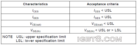
通过下面的测试,确认下表1中规定的IGBT特性。
Table 1 – Acceptance-defining characteristics
 6.2.1 Collector-emitter voltages (VCES, VCER, VCEX):集电极-发射极电压
6.2.1.1 目的
To verify that an IGBT withstands the rated collector-emitter voltages VCES, VCER or VCEX under specified conditions.文章来源:http://www.igbt8.com/jc/151.html
6.2.1.2 Circuit diagram (see Figure 1):测试电路
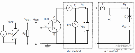 Figure 1 – Circuit for measuring the collector-emitter voltages VCES, VCER, VCEX
6.2.1.3 电路描述
VCC and VGG are the voltage supply. R1 is a circuit protection resistor.
6.2.1.4 测试流程
There are two methods, i.e. the d.c. method and the a.c. method, with circuits according to Figure 1.
The specified conditions between gate and emitter shall be applied. The collector-emitter voltage is set to the specified value.
6.2.1.5 规定条件
– Collector-emitter voltage VCE
– Ambient or case or virtual junction temperature Ta or Tc or Tvj
– VCEX: gate-emitter voltage –VGG
– VCER: resistor connected between gate and emitter
– VCES: short circuit between gate and emitter
6.2.2 Gate-emitter voltage with collector emitter short circuit (±VGES):集电极-发射极短接条件下门极-发射极电压
6.2.2.1 目的
To verify that an IGBT withstands the rated gate emitter voltage ±VGE under specified conditions.
6.2.2.2 电路 (见图2)
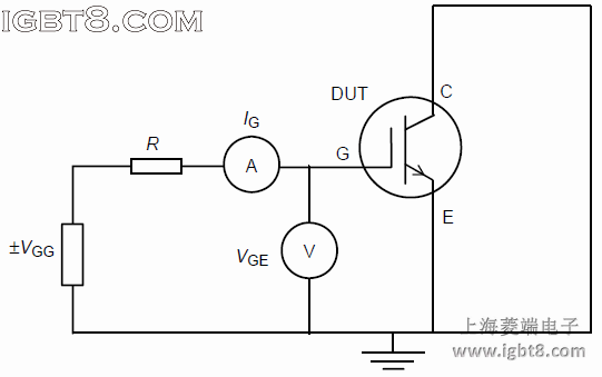 Figure 2 – Circuit for testing the gate-emitter voltage ±VGES
6.2.2.3 电路描述
VGG is the voltage supply. R is a circuit protection resistor.
6.2.2.4 测试流程
The gate-emitter voltage VGE is set to the specified value. A small protective resistor R is to be provided.
6.2.2.5 规定条件
– Ambient or case or virtual junction temperature Ta or Tc or Tvj,环境温度、壳温、结温。
– Gate-emitter leakage current IGES 门极-发射极漏电流
– Short circuit between collector and emitter 短接集电极与发射极
6.2.3 Maximum collector current (IC) 最大集电极电流
6.2.3.1 目的
To verify that the collector current capability of an IGBT is not less than the maximum rated value IC under specified conditions.
6.2.3.2 测试电路 (see Figure 3)
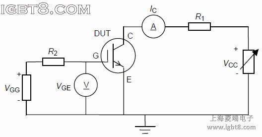 Figure 3 – Circuit for measuring collector current
6.2.3.3 电路描述
VCC and VGG are the voltage supply. R1 is a circuit protection resistor.
6.2.3.4 测试流程
The temperature (Ta or Tc) and the gate-emitter voltage are set and kept to the specified
values. The supply voltage (VCC) is increased until IC reaches the specified value. The
thermal equilibrium might be reached.
6.2.3.5 规定条件
– Ambient or case or virtual junction temperature Ta or Tc环境温度、壳温、结温。
– Collector current IC 集电极电流IC
– Gate-emitter voltage VGE 门极-发射极电压
6.2.4 Maximum peak collector current (ICM):最大峰值集电极电流
6.2.4.1 目的
To verify that the peak collector current capability of an IGBT is not less than the maximum rated value ICM under specified conditions.
6.2.4.2 测试电路 (see Figure 4)
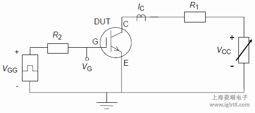 Figure 4 – Circuit for measuring peak collector current
6.2.4.3 测试描述
VCC is the voltage supply and VGG is the gate pulse generator. R1 is a circuit protection resistor.
6.2.4.4 测试流程
The temperature (Ta or Tc or Tvj) and the gate-emitter voltage are set and kept at the specified values. The supply voltage (Vcc) is increased until IC reaches the specified value.
6.2.4.5 规定条件
– Ambient or case or virtual junction temperature Ta or Tc or Tvj 环境温度、壳温、结温。
– Collector current ICM 集电极电流ICM
– Gate emitter voltage, pulse width and duty cycle 门极-发射极电压,脉冲宽度及占空比。
6.1 常规
本文中应用的IGBT测试电路适用于N沟道器件,通过翻转计量表、信号发生器及电源的极性可将该电路应用于P沟道IGBT。
6.2 Verification of ratings (limiting values):额定电压电流参数验证(限值)
通过下面的测试,确认下表1中规定的IGBT特性。
Table 1 – Acceptance-defining characteristics
6.2.1.1 目的
To verify that an IGBT withstands the rated collector-emitter voltages VCES, VCER or VCEX under specified conditions.文章来源:http://www.igbt8.com/jc/151.html
6.2.1.2 Circuit diagram (see Figure 1):测试电路
6.2.1.3 电路描述
VCC and VGG are the voltage supply. R1 is a circuit protection resistor.
6.2.1.4 测试流程
There are two methods, i.e. the d.c. method and the a.c. method, with circuits according to Figure 1.
The specified conditions between gate and emitter shall be applied. The collector-emitter voltage is set to the specified value.
6.2.1.5 规定条件
– Collector-emitter voltage VCE
– Ambient or case or virtual junction temperature Ta or Tc or Tvj
– VCEX: gate-emitter voltage –VGG
– VCER: resistor connected between gate and emitter
– VCES: short circuit between gate and emitter
6.2.2 Gate-emitter voltage with collector emitter short circuit (±VGES):集电极-发射极短接条件下门极-发射极电压
6.2.2.1 目的
To verify that an IGBT withstands the rated gate emitter voltage ±VGE under specified conditions.
6.2.2.2 电路 (见图2)
6.2.2.3 电路描述
VGG is the voltage supply. R is a circuit protection resistor.
6.2.2.4 测试流程
The gate-emitter voltage VGE is set to the specified value. A small protective resistor R is to be provided.
6.2.2.5 规定条件
– Ambient or case or virtual junction temperature Ta or Tc or Tvj,环境温度、壳温、结温。
– Gate-emitter leakage current IGES 门极-发射极漏电流
– Short circuit between collector and emitter 短接集电极与发射极
6.2.3 Maximum collector current (IC) 最大集电极电流
6.2.3.1 目的
To verify that the collector current capability of an IGBT is not less than the maximum rated value IC under specified conditions.
6.2.3.2 测试电路 (see Figure 3)
6.2.3.3 电路描述
VCC and VGG are the voltage supply. R1 is a circuit protection resistor.
6.2.3.4 测试流程
The temperature (Ta or Tc) and the gate-emitter voltage are set and kept to the specified
values. The supply voltage (VCC) is increased until IC reaches the specified value. The
thermal equilibrium might be reached.
6.2.3.5 规定条件
– Ambient or case or virtual junction temperature Ta or Tc环境温度、壳温、结温。
– Collector current IC 集电极电流IC
– Gate-emitter voltage VGE 门极-发射极电压
6.2.4 Maximum peak collector current (ICM):最大峰值集电极电流
6.2.4.1 目的
To verify that the peak collector current capability of an IGBT is not less than the maximum rated value ICM under specified conditions.
6.2.4.2 测试电路 (see Figure 4)
6.2.4.3 测试描述
VCC is the voltage supply and VGG is the gate pulse generator. R1 is a circuit protection resistor.
6.2.4.4 测试流程
The temperature (Ta or Tc or Tvj) and the gate-emitter voltage are set and kept at the specified values. The supply voltage (Vcc) is increased until IC reaches the specified value.
6.2.4.5 规定条件
– Ambient or case or virtual junction temperature Ta or Tc or Tvj 环境温度、壳温、结温。
– Collector current ICM 集电极电流ICM
– Gate emitter voltage, pulse width and duty cycle 门极-发射极电压,脉冲宽度及占空比。
服务热线:021-58979561
业务咨询qq:447495955
业务咨询qq:1852433657
业务咨询qq:513845646
技术支持qq:313548578
技术交流群:376450741
业务咨询:
业务咨询:
业务咨询:
技术支持:
媒体合作:
沪ICP备09068927号 igbt8.com版权所有 Copyright 2008-2018
URL:http://www.igbt8.com qq:1852433657 欢迎加入IGBT技术交流群:376450741
技术支持: IGBT应用技术网
URL:http://www.igbt8.com qq:1852433657 欢迎加入IGBT技术交流群:376450741
技术支持: IGBT应用技术网