热销产品
准确计算IGBT模块死区时间(2)
2 计算合适的死区时间
如上所述,死区时间一方面应该满足避免桥臂直通的要求,另一方面死区时间应尽可能的小以确保电压源逆变器正常工作。所以这里的一大挑战是为专用IGBT器件和IGBT驱动找到一个合适的死区时间。文章来源: http://www.igbt8.com/qd/170.html
2.1 死区时间计算基础
For calculation of control dead time we use the following equation:

Td_on_min : the minimal turn on delay time.最小导通延迟时间
Tpdd_max : the maximal propagation delay of driver.驱动器最大传输延迟时间
Tpdd_min : the minimum propagation delay of driver.驱动器最小传输延迟时间
1.2 : safety margin to be multiplied.
In this equation the first term td_off_max-td_on_min is the difference of the maximal turn off delay time and the minimal turn on delay time. This term describes characteristic of IGBT device itself plus gate resistor which is used. Since fall and rise time is normally very short in comparison with delay time, they will be not considered here. The other term tpdd_max-tpdd_min is the propagation delay time difference (delay time mismatch) which is determined from driver. This parameter will be found normally in datasheet of driver from driver manufacturers. Typically this value is quiet high with opto-coupler based drivers.
Sometimes dead time will be calculated from typical datasheet values just multiplying by a safety factor from field experience. This method will work in some cases but is not precise enough in general. With measurements shown here, a more precise approach will be presented.
Because IGBT datasheet only gives typical values for standardized operation condition, it is necessary to obtain the maximal values for dedicated driving condition. For this purpose a series of measurements is done in order to obtain proper value for delay time and then to calculate dead time.
2.2 开关及延迟时间定义
开关及延迟时间定义如下:
td_on : from 10% of Vge to 10% if Ic.
tr : from 10% of Ic to 90% of Ic.
td_off : from 90% of Vge to 90% of Ic.
tf : from 90% of Ic to 10% of Ic.
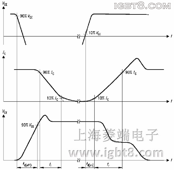
Figure 3 Definition of switching times.
2.3 IGBT门极电阻及驱动器输出阻抗的影响门极电阻设置会显著地影响开关延迟时间,一般来说,电阻越大则延迟时间越长。推荐在实际应用的门极电阻条件下测量延迟时间。典型的开关时间对门极电阻的关系图如下图所示:
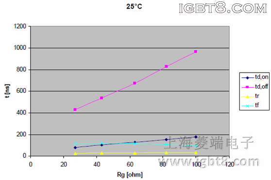
Figure 4 Switching times vs. Rg @25°C
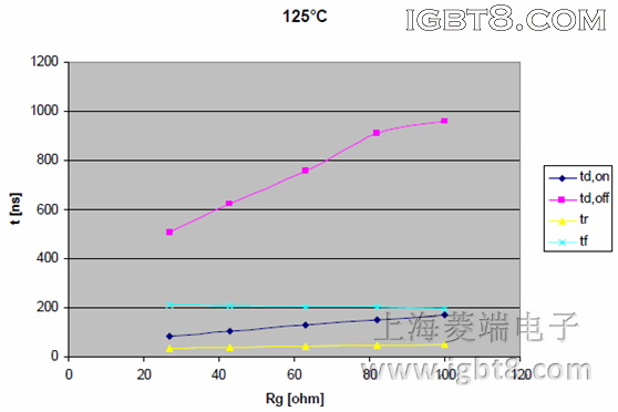
Figure 5 Switching times vs. Rg @125°C
All tests were done with FP40R12KT3 module, gate voltage is -15V/+15V, DC link voltage is 600V and switched current is nominal current of 40A.服务热线:021-58979561
业务咨询qq:447495955
业务咨询qq:1852433657
业务咨询qq:513845646
技术支持qq:313548578
技术交流群:376450741
业务咨询:
业务咨询:
业务咨询:
技术支持:
媒体合作:
沪ICP备09068927号 igbt8.com版权所有 Copyright 2008-2018
URL:http://www.igbt8.com qq:1852433657 欢迎加入IGBT技术交流群:376450741
技术支持: IGBT应用技术网
URL:http://www.igbt8.com qq:1852433657 欢迎加入IGBT技术交流群:376450741
技术支持: IGBT应用技术网