热销产品
IGBT模块电路杂散电感测量方法
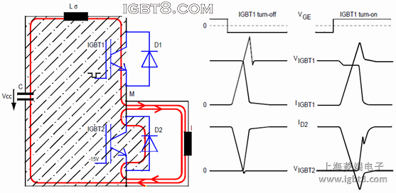
图1为IGBT半桥拓扑电路图,及当开关IGBT1时产生的电压电流波形。该电路杂散电感Ls代表所有的分布电感(电容器,母线和IGBT模块)。
换流回路的杂散电感可以通过IGBT在开通时的两端压降获得:当IGBT依然处于阻断状态,而电流已经开始上升时,可以测量di/dt及电压降DV,根据测量值计算电感值,见下式:
Ls = DV / di/dt.
i: 400A / div (green) v: 200V / div. (black)
该电压降发生的时刻,二极管仍然没有阻断能力。因此电压降只能是由杂散电感产生,不需考虑其他的影响。The circuit stray inductance is calculated according to the above shown formula at zero
crossing of current. We get the following values:
DV » 230V
di/dt » 3200A/800ns
Å Ls » 58nH
Fig.1: Half-bridge circuit with current and voltage waveforms when switching IGBT1
Due to the changing current a voltage drop of Ls * dioff/dt occurs across the stray inductance Ls. It is overlayed to the DC link voltage VCC and seen as a voltage spike across the turning-off IGBT1. According to the RBSOA diagram, this spike must be limited to the blocking voltage VCES of the IGBT module (measured at the chip, means measured at the CE auxiliary terminals). Also a derated curve is given in the data-sheet for measurements at the power terminals, taking into account the internal module stray inductance between main and auxiliary terminals of the module.文章来源:http://www.igbt8.com/il/150.html换流回路的杂散电感可以通过IGBT在开通时的两端压降获得:当IGBT依然处于阻断状态,而电流已经开始上升时,可以测量di/dt及电压降DV,根据测量值计算电感值,见下式:
Ls = DV / di/dt.
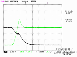
Fig.2: Switching curves of current and voltage when turning on an IGBT
Example:i: 400A / div (green) v: 200V / div. (black)
该电压降发生的时刻,二极管仍然没有阻断能力。因此电压降只能是由杂散电感产生,不需考虑其他的影响。The circuit stray inductance is calculated according to the above shown formula at zero
crossing of current. We get the following values:
DV » 230V
di/dt » 3200A/800ns
Å Ls » 58nH
服务热线:021-58979561
业务咨询qq:447495955
业务咨询qq:1852433657
业务咨询qq:513845646
技术支持qq:313548578
技术交流群:376450741
业务咨询:
业务咨询:
业务咨询:
技术支持:
媒体合作:
沪ICP备09068927号 igbt8.com版权所有 Copyright 2008-2018
URL:http://www.igbt8.com qq:1852433657 欢迎加入IGBT技术交流群:376450741
技术支持: IGBT应用技术网
URL:http://www.igbt8.com qq:1852433657 欢迎加入IGBT技术交流群:376450741
技术支持: IGBT应用技术网