热销产品
IGBT驱动参数评估十二-二极管关断
5 二极管关断过程分析
可以通过改变一些参数分析二极管的关断行为,下面会详细讨论。为了便于比较,引用了一个典型的测量基准。
5.1 IGBT驱动栅极电阻RG的变化
如图41、42、43所示,增加的门极电阻会对IGBT的开通行为有以下影响:
降低二极管的反向恢复峰值电流Irr
降低di/dt
降低dv/dt
降低二极管关断过程的整体震荡。
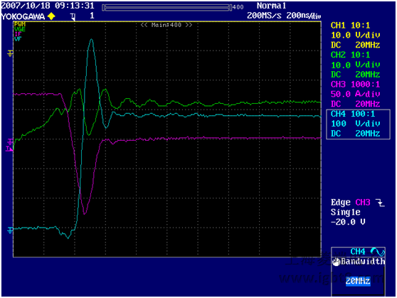
Max(C2): 17.08V, Max(C3): 77A, Max(C4): 638V


如图44、45、46所示,增加的门极发射极电容对IGBT的动作影响如下:
降低二极管的反向恢复峰值电流Irp
降低di/dt
降低dv/dt
降低二极管关断过程的整体震荡。
Chart 8 summarizes the results as function of the gate-emitter capacitor CGE.
Max(C2): 16.66V, Max(C3): 77A, Max(C4): 600V

关于二极管关断过程的开关行为,可以看到,-8V或者0V的负端门极电压对二极管的正向压降VF及正向电流IF没有差别。
Max(C2): 17.08V, Max(C3): 77A, Max(C4): 638V

可以通过改变一些参数分析二极管的关断行为,下面会详细讨论。为了便于比较,引用了一个典型的测量基准。
5.1 IGBT驱动栅极电阻RG的变化
如图41、42、43所示,增加的门极电阻会对IGBT的开通行为有以下影响:
降低二极管的反向恢复峰值电流Irr
降低di/dt
降低dv/dt
降低二极管关断过程的整体震荡。
Max(C2): 17.08V, Max(C3): 77A, Max(C4): 638V
Figure 41: Diode turn-off with RG = 1.8Ω
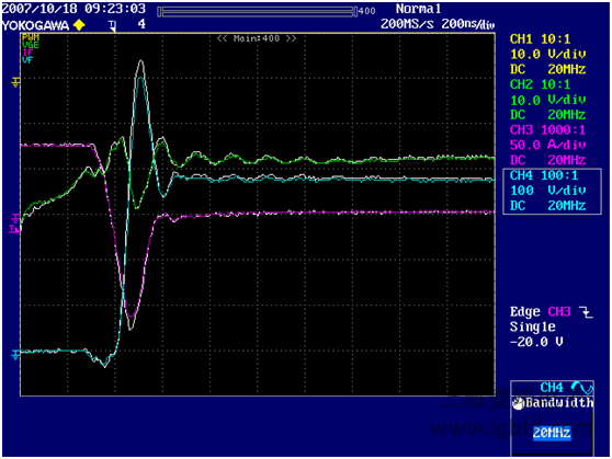
Max(C2): 15.83V, Max(C3): 77A, Max(C4): 521V
Figure 42: Diode turn-off with RG = 3.3Ω
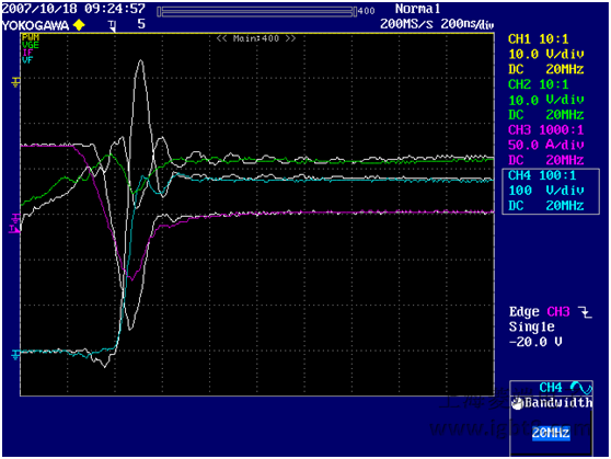
Max(C2): 13.75V, Max(C3): 77A, Max(C4): 404V
Figure 43: Diode turn-off with RG = 6.8Ω
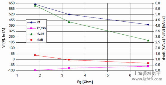
Chart 7 summarizes the results as function of the gate resistor RG.转载请注明出处 http://www.igbt8.com
Chart 7: Vf, Irr,min , dv/dt, and di/dt vs. RG
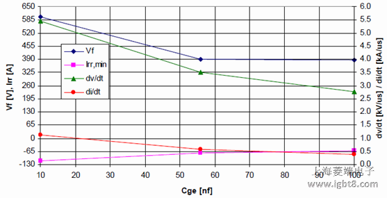
5.3 变化的门极发射极电容CGE如图44、45、46所示,增加的门极发射极电容对IGBT的动作影响如下:
降低二极管的反向恢复峰值电流Irp
降低di/dt
降低dv/dt
降低二极管关断过程的整体震荡。
Chart 8 summarizes the results as function of the gate-emitter capacitor CGE.
Max(C2): 16.66V, Max(C3): 77A, Max(C4): 600V
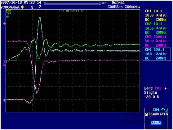
Figure 44: Diode turn-off with RG = 1.8Ω and CGE = 10nF
Max(C2): 13.32V, Max(C3): 77A, Max(C4): 392V
Figure 45: Diode turn-off with RG = 1.8Ω and CGE = 56nF
Max(C2): 12.08V, Max(C3): 75A, Max(C4): 388V
Figure 46: Diode turn-off with RG = 1.8Ω and CGE = 100nF
Chart 8: Vf, Irr,min , dv/dt, and di/dt vs. RG
5.3 变化的负端门极电压VGE,min关于二极管关断过程的开关行为,可以看到,-8V或者0V的负端门极电压对二极管的正向压降VF及正向电流IF没有差别。
Max(C2): 17.08V, Max(C3): 77A, Max(C4): 638V
Figure 47: Diode turn-off with VGE,min = -8V
Max(C2): 16.66V, Max(C3): 77A, Max(C4): 625V
Figure 48: Diode turn-off with VGE,min = 0V
作者:Jackie Zhao
服务热线:021-58979561
业务咨询qq:447495955
业务咨询qq:1852433657
业务咨询qq:513845646
技术支持qq:313548578
技术交流群:376450741
业务咨询:
业务咨询:
业务咨询:
技术支持:
媒体合作:
沪ICP备09068927号 igbt8.com版权所有 Copyright 2008-2018
URL:http://www.igbt8.com qq:1852433657 欢迎加入IGBT技术交流群:376450741
技术支持: IGBT应用技术网
URL:http://www.igbt8.com qq:1852433657 欢迎加入IGBT技术交流群:376450741
技术支持: IGBT应用技术网