热销产品
IGBT参数测试IEC标准一-术语和定义(2)
3.4 IGBT额定值和特性相关术语;IGBT动态参数及特性
3.4.1
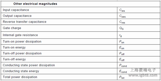
input capacitance:输入电容
Cies
Capacitance between the gate and emitter terminals with the collector terminal short-circuited to the emitter terminal for a.c.
3.4.2
output capacitance:输出电容
Coes
Capacitance between the collector and emitter terminals with the gate terminal short-circuited
to the emitter terminal for a.c.
3.4.3
reverse transfer capacitance:反向传输电容
Cres
Capacitance between the collector and gate terminals
3.4.4
gate charge:门极电荷
QG
Charge required to raise the gate-emitter voltage from a specified low to a specified high level
3.4.5
internal gate resistance:内部门极电阻
rg
Internal series resistance
3.4.6
turn-on energy (per pulse):开通损耗(每脉冲)
Eon
Energy dissipated inside the IGBT during the turn-on of a single collector current pulse.
NOTE: The corresponding turn-on power dissipation under periodic pulse conditions is obtained by multiplying Eon by the pulse frequency.文章来源:http://www.igbt8.com/jc/147.html
3.4.7
turn-off energy (per pulse):关断损耗(每脉冲)
Eoff
Energy dissipated inside the IGBT during the turn-off time plus the tail time of a single collector current pulse.
NOTE :The corresponding turn-off power dissipation under periodic pulse conditions is obtained by multiplying Eoff by the pulse frequency.
turn-on delay time:开通延迟时间
td(on), td
Time interval between the beginning of a voltage pulse across the input terminals which switches the IGBT from the off-state to the on-state and the beginning of the rise of the collector current
NOTE: Usually, the time is measured between points corresponding to 10 % of the input and output pulse amplitudes.
3.4.9
rise time:上升时间
tr
Time interval between the instants at which the rise of the collector current reaches specified lower and upper limits, respectively, when the IGBT is being switched from the off-state to the on-state
NOTE :Usually the lower and upper limits are 10 % and 90 % of the pulse amplitude.
3.4.10
turn-on time:开通时间
ton
Sum of the turn-on delay time and the rise time
3.4.11
turn-off delay time:关断延迟时间
td(off), ts
Time interval between the end of the voltage pulse across the input terminals which has held the IGBT in its on-state and the beginning of the fall of the collector current when the IGBT is switched from the on-state to the off-state
NOTE :Usually, the time is measured between points corresponding to 90 % of the input and output pulse amplitudes.
3.4.12
fall time:下降时间
tf
Time interval between the instants at which the fall of the collector current reaches specified upper and lower limits, respectively, when the IGBT is switched from the on-state to the off-state
NOTE:Usually, the upper and lower limits are 90 % and 10 % of the pulse amplitude.
3.4.13
turn-off time:关断时间
toff
Sum of the turn-off delay time and the fall time
3.4.14
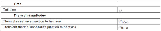
tail time:拖尾电流时间
tz
Time interval from the end of the turn-off time to the instant at which the collector current has fallen to 2 % or lower specified value
4.1 常用
IGBT常用字母符号在IEC 60747-1的条款4里定义。
4.2 另外常用下标
C,c: collector(集电极)
E,e: emitter(发射极)
G,g: gate(门极)
sat: saturation(饱和)
th: threshold(阈值)
Z,z: tail(拖尾)
S: termination with a short circuit(短路端子)
R: termination with a resistor(用电阻连接端子)
X: termination with specified gate emitter voltage(用规定的门射极电压连接端子)
Sus: sustaining(维持)
服务热线:021-58979561
业务咨询qq:447495955
业务咨询qq:1852433657
业务咨询qq:513845646
技术支持qq:313548578
技术交流群:376450741
业务咨询:
业务咨询:
业务咨询:
技术支持:
媒体合作:
沪ICP备09068927号 igbt8.com版权所有 Copyright 2008-2018
URL:http://www.igbt8.com qq:1852433657 欢迎加入IGBT技术交流群:376450741
技术支持: IGBT应用技术网
URL:http://www.igbt8.com qq:1852433657 欢迎加入IGBT技术交流群:376450741
技术支持: IGBT应用技术网