热销产品
准确计算IGBT模块死区时间(3)
2.4 其他参数对IGBT开关时间的影响
Besides the gate resistor values, there are other parameters having significant impact on delay times:
l Collector current.
l Gate drive supply voltage.
2.4.1 IGBT开通延迟时间
To estimate this relationship, a series of measurements was done. First the dependence of turn on delay time and current was investigated. The results are shown in the next figure:文章来源: http://www.igbt8.com/qd/170.html
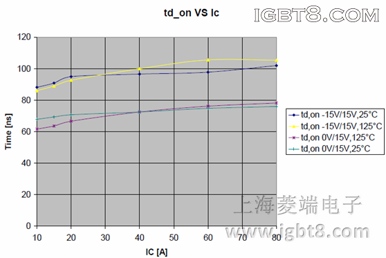
Figure 6 The turn on delay time vs. switched current Ic
All tests were done with a FP40R12KT3 module at a DC link voltage of 600V, gate resistor is chosen according to datasheet value.从结果可以看出,集电极电流IC变化时,开通延迟时间几乎保持不变。-15V/+15V的门极电压下的开通延迟时间比0V/+15V的门极电压条件下要长。但对于进一步的计算控制死区时间,该变化很小可以忽略不计。
2.4.2 关断延迟时间
最大关断延迟时间是计算死区时间最重要的因素。
Since this value determines almost entirely how long the final calculated dead time will be. So we will investigate this delay time in detail.
1. IGBT模块自身产生的开通延迟时间
To answer this question the following test based on a characterization driver board is done in laboratory. The characterization driver board is considered as an optimal driver, which means that this particular driver will cause no delay (which is almost true with an oversized driver), so the whole delay time is considered to be caused by the IGBT device itself. Following block diagram shows test setup:

Figure 7 Block diagram of test with ideal driver
2. 如果IGBT阈值电压在规格书中有最小值,最大关断延迟时间是多少?(反映了模块与模块之间Vth的 )To answer this question an additional diode is connected to simulate the reduced Vth voltage. The diode has a voltage drop of approximately 0.7…0.8V, which is quite similar to the Vth variation of FP40R12KT3 module. Following block diagram shows principle test setup:
要回答此问题,连接了一个额外的二极管以模拟降低的Vth电压,该二极管大约有0.7V…0.8V的压降,与IGBT模块FP40R12KT3的Vth漂移相似。下图为试验装置原理:
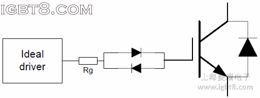
Figure 8 Block diagram of the test to simulate variation of Vth in worst case.
3. IGBT 驱动器输出级对开关时间的影响?市场上的驱动器可分为两类,一种是MOSFET晶体管输出级,另一种是双极晶体管输出级。
为了模拟MOSFET输出级,额外连接了一个电阻作为MOSFET的通态电阻Rds(on),模拟Vth变化的二极管保留,下图为试验装置原理:
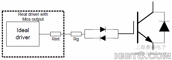
Figure 9 Block diagram of test to simulate variation of Vth and driver with mosfet output.
4. 双极晶体管输出级驱动器的影响?To answer the question an additional diode which simulated the voltage drop on bipolar transistor within output stage was connected. The following block diagram shows principle test setup:
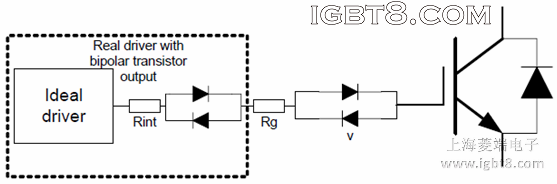
Figure 10 Block diagram of the test to simulate the variation of Vth and driver with bipolar transistor output
With the configurations shown above the measurement of turn off delay time was done in our laboratory with module FP40R12KT3 and driver board which had been considered as optimal. Test conditions were Vdc=600V, Rg=27Ω. Results are shown in the next two figures:
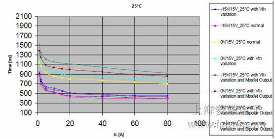
Figure 11 Turn off delay time vs. Ic @25°C

Figure 12 Turn off delay time vs. Ic @125°C
从结果可以看到,关断延迟时间随着开关电流的降低会有明显的增加。因此,简单的根据选择的门极电阻计算死区时间显然不够精确。在专用的驱动条件下测量延迟时间然后根据测量值计算死区时间是更好及更精确的方法。通常测量1%常规电流条件下的延迟时间,足以计算需要的死区时间。另一个需要考虑的方面是,关断延迟时间在0V/+15V驱动电压条件下会增加,0V/+15V电压时驱动输出级的影响也较大,意味着若用0V/+15V开关电压则需要慎重选择驱动器。另外,较低的开关断集电极电流IC会增加关断时间td_off也应当被考虑。
服务热线:021-58979561
业务咨询qq:447495955
业务咨询qq:1852433657
业务咨询qq:513845646
技术支持qq:313548578
技术交流群:376450741
业务咨询:
业务咨询:
业务咨询:
技术支持:
媒体合作:
沪ICP备09068927号 igbt8.com版权所有 Copyright 2008-2018
URL:http://www.igbt8.com qq:1852433657 欢迎加入IGBT技术交流群:376450741
技术支持: IGBT应用技术网
URL:http://www.igbt8.com qq:1852433657 欢迎加入IGBT技术交流群:376450741
技术支持: IGBT应用技术网